LSTM Accelerator: RTL-to-GDSII ASIC Implementation
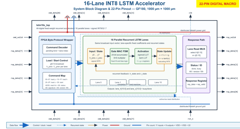
The main design constraint was the 22-pin macro boundary. I used a byte-command interface to load data, start computation, read status, and return lane results without exposing the parallel internal datapath at the chip boundary.
16 parallel lanesINT8 / Q1.722-pin macro10 MHz post-route
Datapath and control
Sixteen lanes operate on INT8 / Q1.7 data. Each lane contains a signed 8 × 8 MAC, LUT-based sigmoid and tanh functions, and registers for cell and hidden state. A controller sequences the input, forget, candidate, and output gates.
RTL verification
I generated reference vectors with a Python model and compared them against SystemVerilog simulation. The tests cover command sequencing, lane execution, state updates, signature behavior, and result readback.
GF180MCU implementation
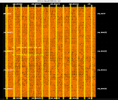
The design went through synthesis, floorplanning, placement, clocking, routing, and post-route analysis in the LibreLane/OpenROAD flow. The completed macro reached 10 MHz post-route and passed DRC, LVS, XOR, antenna, IR-drop/EM, and multi-corner timing checks.
SystemVerilog · Python · LibreLane · OpenROAD · GF180MCU · STA